
Conductors, Insulators and Semi-conductors
- An insulator is a material or object which resists flow of heat (thermal insulator) or electrical charges (electrical insulators ). Examples are paraffin, wood, rubber, plastics etc.
- Conductors are materials that contain free electrons which carry an electrical charge from one point to another. Examples are metals and non-metals like carbon, graphite etc.
- Semi-conductors are materials or objects which allow the flow of electrical heat or energy through them under certain conditions i.e. temperature. Examples are germanium, silicon, cadmium sulphide, gallium arsenide etc.
Electronic Bond Structure
- This is the series of allowed or forbidden bands that it contains according to the band theory which postulates the existence of continuous ranges of energy values (bands) which electron may occupy “allowed” or not occupy ‘forbidden”.
- According to molecular orbital theory, if several atoms are brought together in a molecule, their atomic orbitals split, producing a number of molecular orbitals proportional to the number of atoms.
- However when a large number of atoms are brought together the difference between their energy levels become very small, such that some intervals of energy contain no orbitals and this theory makes an assumption that these energy levels are as numerous as to be indistinct.
Number, Size and Spacing of Bands
- Any solid has a large number of bands (theoretically infinite). Bands have different widths based upon the properties of the atomic orbitals from which they arise.
- Bands may also overlap to produce a bigger single band.
Valence and Conduction Bands
- Valence band is the highest range of electron energies where electrons are normally present at zero temperature.
- Conduction band is the range of electron energy higher than that of the valence band sufficient to make electrons free (delocalized) ; responsible for transfer of electric charge. Insulators and semi-conductors have a gap above valence band followed by conduction band above it.
- In metals, the conduction band is the valence band.
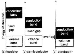
Band Structure of a Semi-conductor
- Electrons in the conduction band break free of the covalent bonds between atoms and are free to move around hence conduct charge.
- The covalent bonds after the electrons have moved.
- The current carrying electrons in the conduction band are known as free electrons.

Doping of Semi-conductors
- Doping is the introduction of impurities in semi-conductors to alter their electronic properties.
- The impurities are called dopants.
- Doping heavily may increase their conductivity by a factor greater than a million.
Intrinsic and Extrinsic Semi-conductors
- An intrinsic semi-conductor is one which is pure enough such that the impurities in it do not significantly affect its electrical behavior.
- Intrinsic semi-conductors increase their conductivity with increase in temperature unlike metals.An extrinsic semi-conductor is one which has been doped with impurities to modify its number and type of free charge carriers present.
N-type semi-conductors
- In this case the semi-conductor is given atoms by an impurity and this impurity is known as donor so it is given donor atoms (donated).

P-type semi-conductors
- The impurity within the semi-conductor accepts atoms with free electrons (dopants).
- This forms a ‘hole’ within-conductors.

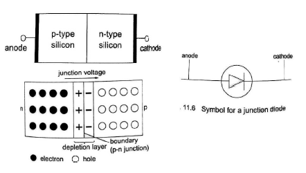
Junction Diodes
- Junction refers the region where the two types of semi-conductors meet .
- The junctions are made by combining an n-type and p-type semi-conductor.
- The n-region is the cathode and the p-region is the anode.
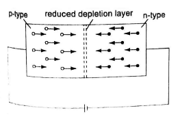
Forward bias of a p-n junction
- It occurs when the p-type block is connected to the positive terminal and the n-type block is connected to the negative terminal of a battery.
- The depletion layer of the junction reduces to be very thin to allow the flow of electric current.
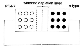
Reverse bias of a p-n junction
- The negative terminal of the battery is connected to the p-type region while the n-type is connected to positive terminal.
- The depletion layer widens and resists the flow of electrons to minimal or zero (no currentflowing through) when the electric field increases beyond critical point the diode junction eventually breaks down and at this voltage it is referred to as the breakdown voltage.
- Diodes are intended to operate below the breakdown voltage.
Applications of Junction Diodes
- They are mainly used for rectification of a.c. current for use by many electrical appliances.
- Rectification is the conversion of sinusoidal waveform into unidirectional (non-zero) waveform.
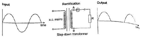
Half Wave Rectification
- In this case the first half cycle of a sinusoidal waveform is positive and the inclusion of a reverse biased diode makes the current not to flow to the negative side of the wave.
- The current therefore conducts on every half cycle hence a half wave rectification is achieved.
- The voltage is d.c. and always positive in value though it is not steady and needs to be smoothed by placing a large capacitor in parallel to the load as shown.
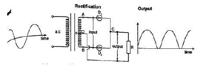
Two Diodes and Centre-tap Transformer Full Wave Rectification
- This is achieved by using a transformer whose output has a centre tap that is taken at two points where one is half the other as shown.
- Two diodes are connected in such a way that each conducts a current through the load resistor during a particular half cycle.
- During the first half-cycle D1, is forward biased while D2, is reverse biased. Hence, the path taken by the current is AD1, CO. During the next half-cycle, D2, is forward biased while D1, is reverse biased and the path of the current is BD2, CO.
- Notice that during both half-cycles, current flows through the resistor in the same direction.
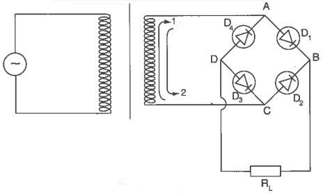
Bridge full Wave Rectification
- In this case a bridge rectifier is used to achieve a full wave rectification.
- During the first half-cycle, point A is positive with respect to C, hence D1, and D3, are forward biased while D2, and D4, are reverse biased. The path of the current is thus ABDCA. During the second half-cycle, point A becomes negative with respect to C and diodes D2, and D4, become forward biased while D and D, are reverse biased. The path of the conventional current is then CBDAC.
- Notice that during both half-cycles, current flows through the load resistor R, in the same directions.
Some advantages of the bridge rectifier are:- a smaller transformer can be used, because there is no need for centre-tapping.
- it is suitable for high voltage regulation.
- In general, the full-wave rectifier gives a stronger and smoother output than the half-wave rectifier. If a capacitor is connected across the resistor, the rectified output is smoothened.
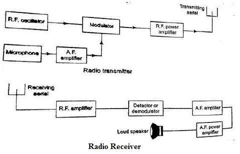
Radio Transmitter and Receiver
- Radio waves are produced by circuits that make electrons vibrate and they are known as oscillators which produce varied frequencies.
- Since radio waves have greater range in air than sound or even light waves they are used as carriers of audio (sound) and visual information (TV) waves.
- The sound is first changed into electrical vibrations by use of a microphone or other device then added to the radio carrier wave and this changes the amplitude of the carrier and is called amplitude modulation.
- The modulated wave is given out by the transmitting aerial and received by another aerial in a radio or TV when they cause vibrations between the earth and the aerial.
- They are then demodulated by a diode and hence heard as a sound or image.
Join our whatsapp group for latest updates
Tap Here to Download for 50/-
Get on WhatsApp for 50/-
Download ELECTRONICS - Form 4 Physics Notes.
Tap Here to Download for 50/-
Get on WhatsApp for 50/-
Why download?
- ✔ To read offline at any time.
- ✔ To Print at your convenience
- ✔ Share Easily with Friends / Students